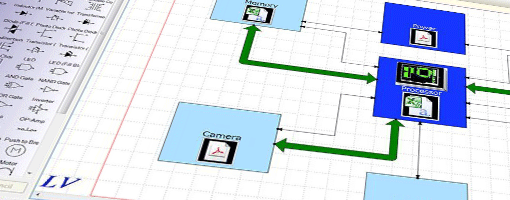
Describe the logical architecture of your system using functional blocks and design reuse modules
System Planner provides a system-level design environment for the architectural planning and optimization of electronic systems and products. It enables engineers to optimize partitioning and performance of multi-board systems and maximize design reuse, while eliminating the need to re-enter up-front planning data into the design tools during detailed design.

Describe the logical architecture of your system using functional blocks and design reuse modules

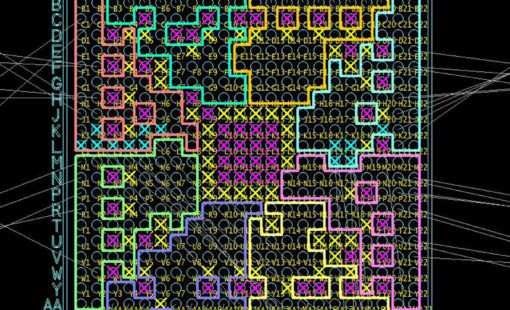
Finalize the PCB partitioning and floor planning of single and multi-board systems

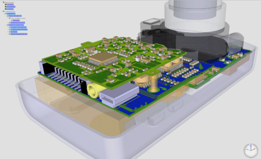
Represent your single and multi-board systems in 3D to check the fit of the boards in the enclosure

Analyze parametric values of components and nets to optimize part use, cost and availability
Take a look at our video and get an overview of System Planner's comprehensive capabilities in 3:20 min
System Planner is the first solution in the industry to support complete upfront architecture of your electronics products. It is the starting point for concept development and design creation. Steps that were once disconnected are now intelligently brought together in one view. Engineers and designers can flow through the design process optimizing form, fit and function of single and multi-board systems, maximizing design reuse, without reentering upfront planning data into the design tools during detailed design.
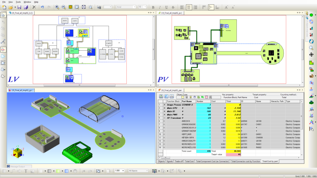
System Planner provides optimization and validation of your design across four domains: functional, PCB, mechanical and parametric requirements.
System Planner fully supports modular design. The functional design can begin with your previous generation schematic. Simply draw a functional block and attached the schematic. Icons on each block will indicate the block’s content. Additional blocks can be added directly from your corporate library which are typically used for modular design or design reuse. Functional blocks can also contain a parts list if the detailed design is not complete. The parts list can contain a few required parts along with prices, weight, power consumption, etc. Or a functional block can be a place holder with the intent to have the contents defined during detailed design.
Many products or systems today are comprised of multiple PCBs. For an optimal architecture those boards need to be designed as an entire system and not independent boards. The Physical Visionary enables multi-board partitioning, planning and validation. Begin with your initial assumptions – 3 boards and 3 board outlines. Simply drag the functional blocks from the functional design onto the desired board. You can move functional blocks from board to board anytime. System Planner will tell you how much surface space is being utilized for a routability assessment. After some analysis, you determine that the design can fit on 2 boards which lowers cost dramatically.
To perform a mechanical fit check the mechanical enclosure can be imported from any number of popular MCAD tools including Siemens NX, PTC Creo, Solid Edge, SolidWorks, etc. And you always have the option of directly loading a STEP file. The boards from the Physical Visionary are dragged into the Geometric Visionary where they can be placed within the enclosure. The fit can be inspected along with some clearance and conflict. The PCB shape can be modified at this time to meet a clearance requirement. That board shape change automatically propagates back to the PCB planning tool.
The Parametric Visionary maintains an up to date report as the design evolves. As the systems engineer adds design modules, the BOM, cost, weight and any other listed parameter is automatically updated accordingly. Requirement targets for cost or weight can also be set. As the design is evolving, the design team can see actual cost and weight compared to design requirements.
A powerful capability of System Planner is to move the functional and multi-board PCB design directly into Design Gateway (schematic design) and Design Force (PCB design) respectively. Unlike other PCB design systems, Design Gateway and Design Force support system or multi-board design processes. The multi-board system is maintained and managed throughout the detailed design process. The product or system that you have optimized and validated in System Planner moves directly into the detailed design process without any data re-entry.
The following can be added to extend the functionality of System Planner
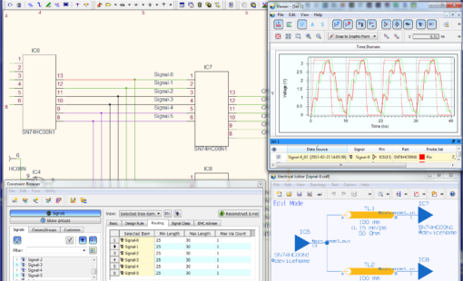
Scenario EX enables to check the electrical characteristics and the connection topology of signal tracks. It allows “What-If Scenarios” of both schematic and layout data to optimize the behaviour of a circuit. It can be used both for interactive design and design verification.
PCB Design Creation - Design Gateway is a platform for logical circuit design and verification of single and multi-board system-level electronic designs. It supports a true system-level circuit design in which individual circuits can be represented and connected as blocks.
Design Force combines traditional 2D design with native 3D design and the latest human interface techniques, accelerated graphics and almost instantaneous rendering and refreshing. It is the fastest, most effective PCB design solution available today. Design Force enables design teams to layout their designs in the context of a complete system or product.
Zuken’s engineering data management platform DS-CR has been created to support the specific demands of PCB design data management. It combines multi-site library, design data and configuration management into a unified engineering environment.
Find out more about CR-8000 System Planner via our webinars, blogs, press releases and more...
This webinar showcases how a leading-edge hardware design process bridges the challenging gaps that occur between analysis and layout design.
This webinar will explore the architecture optimization process using functional design, PCB planning, space planning, and parametric targets. Learn how architecture optimization can improve your product design quality.
See how System Planner helps optimize your designs on an architectural level before committing to detailed design
Many products or systems today are comprised of multiple PCBs. For an optimal architecture those boards need to be designed as a single system and not independent boards. The Physical Visionary enables multi-board partitioning, planning and validation.
Begin with your initial assumptions – 3 boards and 3 board outlines. Simply drag the functional blocks from the functional design onto the desired board. You can move functional blocks from board to board anytime. System Planner will tell you have much surface space is being utilized for a routability assessment. After some analysis, you determine that the design can fit on 2 boards which lowers cost dramatically.
