On-demand webinar
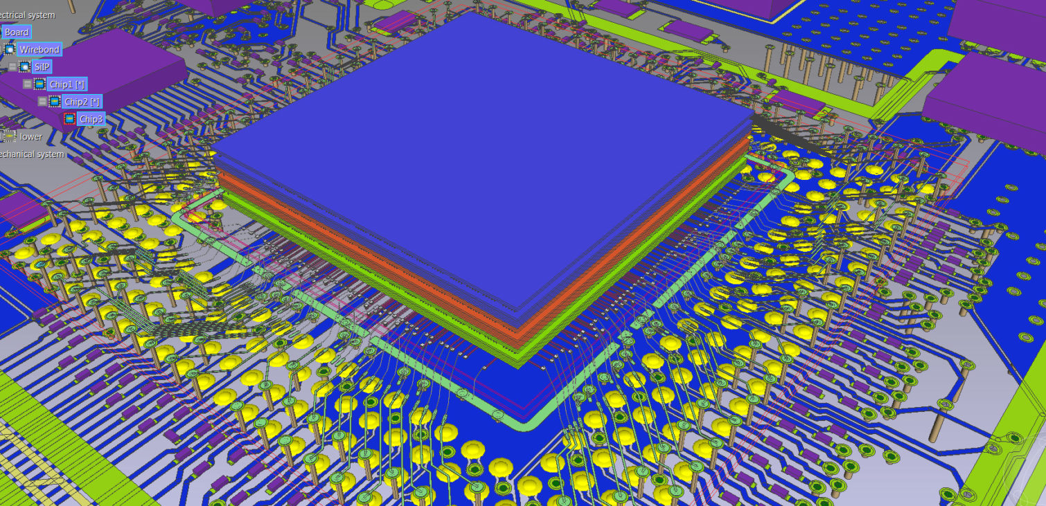
SoCs and advanced packages (such as system-in-package or package-on-package), and the board layout are typically designed in separate environments. Information can be communicated and exchanged from SoCs across different toolsets using file formats such as OpenAccess and LEF/DEF. But due to the continued challenges of higher densities, miniaturization and reduced power consumption, design teams are finding it difficult to consider the complete system when they make critical decisions at each design stage.
This webinar is aimed to help the audience identify disconnects in the chip, package, and board design environment; and explore methods to optimize interconnects, improve design collaboration, and enable signal traceability and analysis across the complete system.
What you will learn:
- A method to help reduce design iterations
- Identify disconnects or manual steps in the design environment
- How to achieve accurate and optimized system level interconnects
- Minimize costly data exchanges
Who should watch:
- Design engineers
- Packaging engineers
- PCB engineers
- Engineering managers
- Product managers
