Webinar: Phased Array or Multi-Channel PCB Design
On-Demand Coming Soon
Menu
Phased array PCB design by Zuken and Sierra
Zuken USA and Sierra Circuits are joining forces to offer you a webinar on the hot topic of phased array PCB design.
Antenna integration is a critical aspect of RF PCB design as it significantly impacts the performance and reliability of the final product. Antennas should operate with sufficient radiation intensity to ensure compliance with industry standards. Identify potential challenges in the layout phase and implement preventative measures and streamline the fabrication process.
In this webinar, you’ll learn how to overcome common issues associated with antenna integration.
Challenges in integrating antennas and ways to resolve them
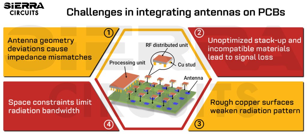
Incorrect stack-up design might increase signal attenuation and reduce antenna radiation intensity. Place high-frequency signal layers close to their reference planes to minimize the signal loop area, preferably one dielectric layer away. Choose materials with low dielectric constant (Dk) and low loss tangent, such as PTFE, ceramic-filled PTFE, and high-speed non-PTFE, for better performance.
Deviations in the antenna geometry can lead to impedance discontinuities and signal reflections.
Use EM simulation tools to model the antenna’s performance and predict impedance mismatches. To compensate for discontinuities, incorporate matching networks with capacitors, inductors, and transmission line sections.
Space constraints on PCBs often limit radiation bandwidth, particularly in compact designs such as mobile devices and IoT applications. When space is limited, choose antennas with multiple frequency bands to combine various functionalities like Wi-Fi (2.4 GHz to 5 GHz) and cellular bands (700 MHz to 2.6 GHz).
You can implement zigzag antenna traces instead of a straight line to save board area. For example, a straight-line antenna designed for 900 MHz may require a length of 83 mm to achieve the desired electrical properties. The same electrical length can be maintained by meandering this line while fitting the antenna into a much smaller area, such as 20 mm x 20 mm.
Rough copper surfaces might increase the effective resistance, leading to greater signal losses and a distorted radiation pattern. Board manufacturers employ plasma treatment and rolled annealed copper foils to address this issue. Profilometers and advanced microscopes can measure surface roughness and ensure it doesn’t affect the radiation pattern.
To prevent the board from overheating, position heat sinks adjacent to the antenna rather than on top. This dissipates heat without affecting the antenna’s tuning and radiation pattern.
Always follow the DFM rules while integrating antennas for reliability. Avoid covering antenna traces with a solder mask, as it can alter the effective dielectric constant and impact signal propagation.
Place antennas away from large metal components, ground planes, and other copper features to avoid interference.
Adhere to regulatory standards such as FCC part 15C, IEEE 802.11, and IPC-2141A to ensure compliance with the industry standards.
What you’ll learn:
● Phased array or multi-channel design requires an optimized process to minimize the time for layout
● Using seed circuits can have many advantages in minimizing the design cycle duration
● Time for edits can also be minimized via an optimized process
● 5 challenges in integrating antennas on PCBs:
1. Antenna geometry deviations cause impedance mismatches
2. Unoptimized stack-up and incompatible material selection lead to signal loss
3. Rough copper surfaces weaken radiation pattern
4. Inconsistent material Dk hinders antenna efficiency
5. Space constraints limit radiation bandwidth
● Addressing thermal issues: heat sink and thermal via placement
● DFM rules for antennas on circuit boards
● Regulatory standards for RF PCBs: FCC part 15C, IEEE 802.11, and IPC-2141A
Date and time:
Wednesday June 26th, 2024
10:00 AM PT
Meet the speakers
Steven Watt
Solutions Architect, Zuken USA, Inc.
Steven Watt is a Solutions Architect for Zuken USA, Inc. In this role he works with customers on implementation and training as well as with development for software direction. He has more than 35 years of experience in the Printed Circuit Board Design industry with an emphasis on IC Packaging technologies. Over the course of his career, he has excelled in roles as a Core Competency applications engineer, Technical Marketing engineer, PCB/MCM/Packaging designer, CAD librarian and Mechanical designer. Steve has a diverse work background including several EDA companies, Boeing, Motorola, and McDonnell Douglas.
Amit Bahl
Chief Revenue Officer, Sierra Circuits
Amit Bahl, widely recognized as the PCB Guy, currently serves as the Chief Revenue Officer at Sierra Circuits. He earned his Bachelor of Science in Engineering from UCLA in 1997, launching his career in Silicon Valley’s tech industry. In 2009, he assumed the role of Director of Sales and Marketing at Sierra Circuits, with a dedicated focus on democratizing design for manufacturing best practices and guidelines for PCB designers and engineers.
Within a short span, Amit successfully propelled Sierra Circuits to become a leading educational platform for all aspects of PCBs. Under his leadership, Sierra expanded to offer blogs, design guides, webinars, calculators and design tools, and a vibrant forum, SierraConnect. Amit remains committed to ensuring the community has access to the essential resources, whether they are developing standard products or boards with specifications for medtech or military applications.
Assuming the position of Chief Revenue Officer since 2022, Amit’s mission persists: to simplify the PCB design journey for all stakeholders. His unwavering dedication continues to drive Sierra Circuits as a trusted resource for the PCB design community.
Related Products & Resources

- Products
September 27, 2023
E3.series Release 2023
E3.series, E3.series Release 2022

- Products
April 23, 2023
Electrical Library & Data Management Software
E3.series

- Products
October 24, 2018
E3.series
E3.series is a Windows-based, scalable, easy-to-learn system for the design of wiring and control systems, hydraulics and pneumatics. The out-of-the-box solution includes schematic (for circuit and fluid diagrams), cable (for advanced electrical and fluid design), panel (for cabinet and panel layout), and formboard (for 1:1 wiring harness manufacturing drawings). Integrated with MCAD, E3.series is a complete design engineering solution from concept through physical realization and manufacturing output.
Read now
E3.series

- Brochure
March 06, 2018
DS-E3 Overview: Next Generation Design Data Management for E3.series
Brochure