Zuken CR-8000 2018 Boosts Process Efficiency in Advanced Single and Multi-board PCB Design
Front-loading of design intent and enhanced auto/interactive placement and routing boost performance, quality and manufacturability
11 July 2018 – Munich, Germany and Westford, MA, USA – The latest release of Zuken’s system-level PCB design environment, CR-8000, has received numerous enhancements aimed at ensuring performance, quality and manufacturability.
Today’s most advanced PCB technologies including high-density and high-speed, multi-board designs, have unique requirements. CR-8000 2018 has delivered new solutions to address these requirements.
CR-8000 is the industry’s most advanced PCB design environment with true system-level engineering and 2D/3D multi-board implementation capabilities. The CR-8000 family of applications spans the complete PCB engineering lifecycle: from system level planning through implementation and design for manufacturability. The CR-8000 environment also includes 3D IC packaging and chip/package/board co-design.
Front-loading of design intent
The focus of CR-8000 2018 is on enabling efficient front-loading of design constraints and specifications to the design creation process, coupled with sophisticated placement and routing capabilities for physical layout. This will increase efficiency and ensure quality through streamlined collaboration across the PCB design chain.
“With current and future smart applications continuing to add complexity to the product design process, controlling adherence of PCB designs to engineering and manufacturing specifications is a critical activity in today’s advanced PCB design projects that takes away valuable time from all domain experts involved,” says Humair Mandavia, Chief Strategy Officer, Zuken Inc. “By providing more intelligent and automated features necessary to drive specification and communication of constraints and guidelines, Zuken wins back valuable time at all points in the PCB design chain, while ensuring maximum quality and reliability.”
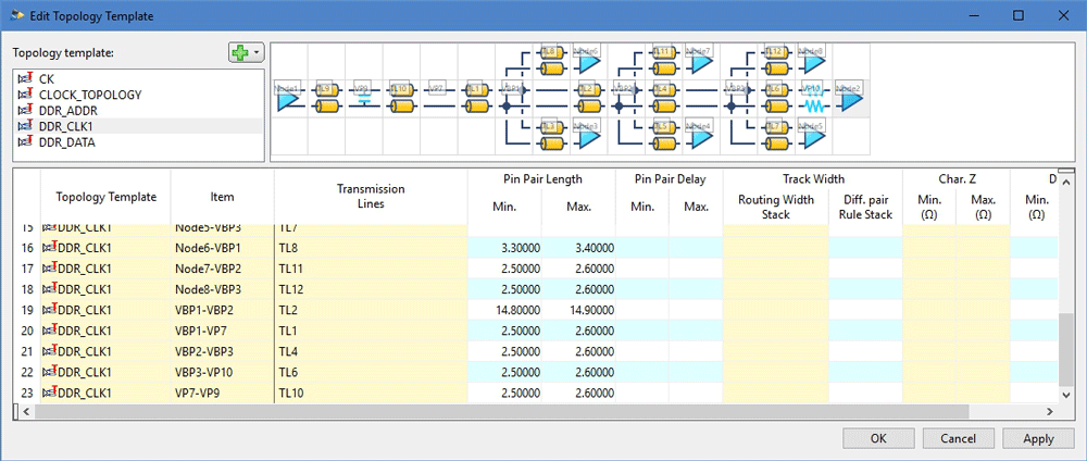
Front-loading of design intent from Design Gateway to Design Force has been achieved by adding an enhanced, unified constraint browser for both applications. This enables hardware engineers to assign topology templates, modify differential signals and assign clearance classes to individual signals. Using a rule stack editor during the circuit design phase, hardware engineers can now load design rules that include differential pair routing and routing width stacks directly from the design rule library into their schematic. Here they can modify and assign selected rules for improved cross talk and differential pair control. Finally, an enhanced component browser enables component variants to be managed in the schematic, and assigned in a user-friendly table.
Sophisticated placement and routing capabilities
Manual routing is supported by a new auto complete & route function that layout designers can use to complete manually routed traces in an automated way. Designers also have the option to look for paths on different layers while automatically inserting vias.
A new bus routing function allows layout designers to sketch paths for multiple nets to be routed over dense areas. An added benefit is the routing of individual signals to the correct signal length as per the hardware engineer’s front loaded constraints, to meet timing skew and budgets. If modifications to fully placed and routed boards are required, an automatic re-route function allows connected component pins to remain connected with a simple reroute operation during the move process. In all operations, clearance and signal length specifications are automatically controlled and adjusted by powerful algorithms.
Design for manufacturing
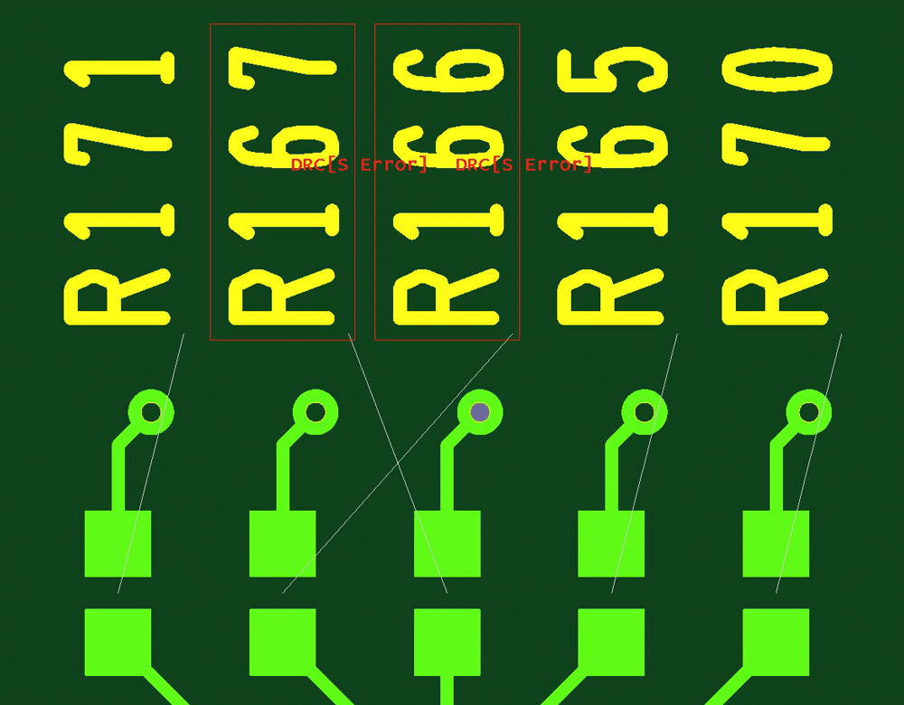
To address manufacturing requirements for high-speed design, the automatic stitching of vias in poured conductive areas can be specified in comprehensive detail, i.e., inside area online, perimeter outline or both inside and perimeter. Design-for-manufacturing (DFM) has been enhanced to include checks for non-conductor items, such as silkscreen and assembly drawing placed reference designators. A design rule check will make sure component reference designators are listed in the same order as the parts for visual inspection accuracy.
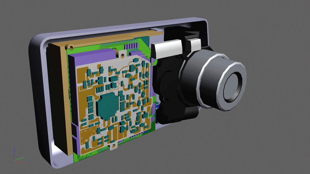
As many product engineers do not work with EDA tools, intelligent PDF documentation is required, especially in 3D. Design Force now supports creation of PRC files commonly used for 3D printing. The PRC files can be opened in PDF authoring applications such as Adobe Acrobat ®, where they are realized as a 3D PDF file complete with 3D models and bookmarks to browse the design.
CR-8000 2018 is available now.
– ends
Related content

- Products
- Products
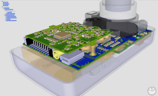
Design Force combines traditional 2D design with native 3D design and the latest human interface techniques, accelerated graphics and almost instantaneous rendering and refreshing. It is the fastest, most effective PCB design solution available today. Design Force enables design teams to layout their designs in the context of a complete system or product.

- Products
Building a competitive product today is much more difficult than a few years ago. Existing PCB-centric design processes are limited to a single PCB and do not provide the necessary tools for today’s competitive product development environment. PCB-centric design processes are falling behind.

