Complex 3D stacked structures and embedded devices
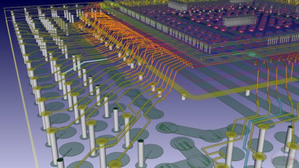
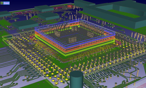
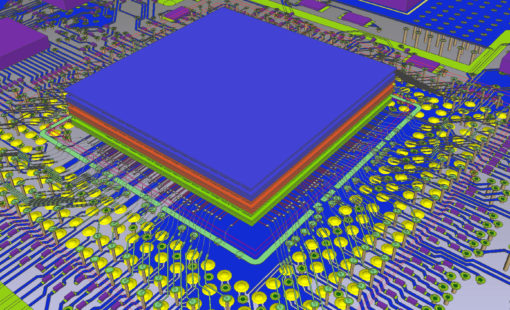
As the industry moves to complex 3D stacked structures and embedded devices, there is a need for tools that can accurately render and provide meaningful visual and DRC feedback to enable rapid right-the-first-time designs.
We can help you with
-
Advanced IC Packaging
-
Chip, package and board co-design for realtime 3D hierarchical design allows design teams to concurrently create any combination of advanced stack dies, packages and PCBs.
-
System Level Circuit Engineering
-
Perform multi-level SI simulation for upfront verification of signal quality issues and determination of optimal termination and topology rules.
-
3D Multi-Board PCB Design
-
You can select between a combination of PCBs, packages, and SoCs into one design and complete the layout of the design as a complete system.
Demonstration
More on Chip-package-board-co-design solutions
Check our latest webinars, white papers, blog posts and more

- Press Release
- On-Demand Webinar
- White Paper
- Press Release
- Press Release
Related products and extensions
- Products
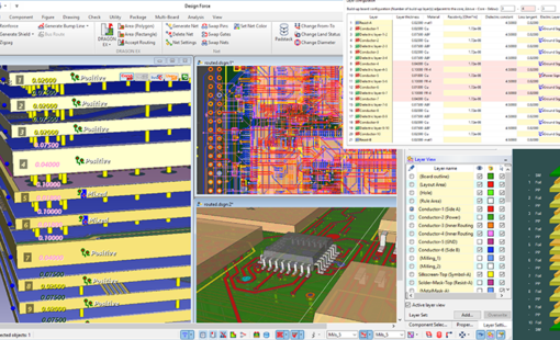
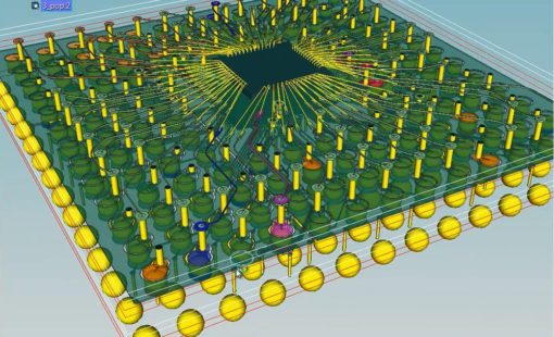
Design Force offers an intuitive, integrated environment for designing single and multi-die packages for wire-bond, flip-chip, and high density advanced packaging. Designers can start designs with early prototype input of chip and package data from the library, reuse data from IC layout tools, and take advantage of parametric wizards to streamline the creation of the system

- Solutions
- Products
- Products
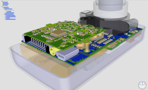
Design Force combines traditional 2D design with native 3D design and the latest human interface techniques, accelerated graphics and almost instantaneous rendering and refreshing. It is the fastest, most effective PCB design solution available today. Design Force enables design teams to layout their designs in the context of a complete system or product.
